Internet Alarm Clock Front Panel

After completing my clinical engineering internship hours while simultaneously working on my research, followed by a three-month research sprint and thesis draft, it’s time for a catch-up post.

An early sketch of the front panel design (Jan 7, 2017).

I started the ball rolling on the Internet Alarm Clock in early 2017 by designing a front panel PCB that implements the alarm clock’s physical user interface (UI).

The front panel is intended to connect to another PCB (to be designed) via a single 6 pin, 0.1″ pitch IDC connector for the I2C (data) bus, power, and button interrupt signal.

Here’s a rundown of the UI elements:

  • Classic red seven-segment display for displaying the time.
  • Character LCD screen for displaying additional information. Transflective with RGB backlight.
  • Four directional buttons (up, down, left, right) for setting the time.
  • Three buttons at the top, each colour-coded for association with a specific functionality:
    • Red, associated with the clock (to match the red seven segment display)
    • Green, associated with the weather reporting functionality (to match the colour of… grass I guess!)
    • Blue, associated with the next arriving bus (inspired by the blue lights on TTC buses)
Alarm clock front panel PCB schematics (Jan 24, 2017)

The front panel electronic design is fairly straightforward. An as1115 does the heavy lifting by doing three things:

  1. Driving the four-digit, seven-segment clock display
  2. Controlling the Newhaven character LCD (NHD-C0220BIZ-FS(RGB)-FBW-3VM
    ) backlight via three switching BJTs (to accommodate the different rated voltages of each of the red, green, and blue backlight LEDs).
  3. Reading the button input from the seven buttons.
Finalized front panel layout (Jan 24, 2017)

For the final layout I decided to move the up/down/left/right buttons alongside the seven-segment display, hoping to make setting the alarm (or, in the absence of Wi-Fi, setting the time) more intuitive.

Unpopulated front panel PCBs (Feb 9, 2017)

I decided to use an Adafruit ESP8266 Wi-Fi module breakout board (2471) as the Wi-Fi module, due to its wide use among hobbyists for their projects, which I can refer to for help. Adafruit’s version comes with the NodeMCU firmware, which implements a Lua-based scripting engine. As I wrote routines in Lua to exercise the displays and read the buttons on the front panel PCB via the I2C bus, I gradually built up a prototype firmware throughout 2017.

Front panel PCB under control of the Adafruit Huzzah ESP8266 breakout board (assembled Mar 2017, photo taken Apr 2018)

I was able to implement the following features using Lua scripting and appropriate selection of modules for a custom NodeMCU build (built using nodemcu-build.com):

  • Automatic syncronization of time over Wi-Fi using NodeMCU’s Network Time Protocol (NTP) module
  • Wi-Fi connection and alarm status icons
  • Automatic dimming of seven segment display at night
  • Setting the alarm time
  • Setting date and time if no Wi-Fi found (could not fully implement due to memory constraints)
  • Visual portion of the alarm, signified by colour-cycling the LCD backlight

The last feature is pretty cool:

Rise and shine!

But, after a certain point, my scripts ran out of memory. Despite there being 4 MB of flash (less 0.5 MB for the firmware) on the underlying module in which to store the scripts, it seems that the Lua interpreter has to load these text files to RAM to execute, and then the variables (of which many are strings) take additional memory, on top of the interpreter’s RAM footprint. Though I’m not entirely sure how NodeMCU partitions and manages the ESP8266 memory space, it appears that RAM is limited to the order of tens of kilobytes. So I may have to use an external microcontroller and program the user interface in C, where it can execute directly from the micro’s flash memory, and reserve the Lua scripting for the high-level network interfacing (e.g. parsing XML or JSON to get the weather and next bus).

Bill of materials, KiCad design files, and Lua scripts are available in this post’s commit.

New Project: Internet Alarm Clock

The goal for this project is to replace my old alarm clock (pictured above) with something that shows the key information I need to know in the morning. That information is:

  • The time
  • The weather
  • When the next bus is coming

Sure, my phone can do all those things. But it takes time to touch and thumb through the various interfaces, beginning with entering a pattern to unlock the screen. And of course apps exist to put the weather and next bus on my phone’s unlock screen, but this information is still not available at a glance because it requires a button press. Having all the key information – time, weather, next bus – always visible on a dedicated display is convenient because it takes next to no effort to access the information; all I have to do is turn my head.

What I want this alarm clock to have:

  • Ability to get the time from the internet
  • A classic red seven segment clock display visible from across the room. (Red so that it doesn’t interfere with my sleep.)
  • A small transflective character LCD screen to provide additional or clarifying information
  • Alarm functionality so it can wake me up in the morning
  • Ability to function as a classic alarm clock in the absence of a wireless internet connection

Here’s what I don’t want this alarm clock to have:

  • An FM radio, internet audio streaming, or any advanced audio capability beyond having an audible alarm. I don’t use the radio functionality of my existing alarm clock anyways so I might as well reduce the complexity of the design by not including this.
  • A graphic display or touchscreen functionality. Just old fashioned tactile buttons please!
  • The classic digital alarm clock interface that required holding down a “time set” or “alarm set” button while tapping a separate minute or hour advancing button.

In addition to solving a practical need, I am using this project to gain experience in the following technical areas:

  • PCB design – for the internal electronics
  • I2C bus – for the displays and buttons
  • State machines – for writing deterministic and easy-to-modify code
  • Wi-Fi modules – for time synchronization, as well as downloading weather and bus times
  • 3D printing – for the case/enclosure
  • Design for usability – I don’t want to frustrate my future self by creating a difficult to use device

This is a project I’ve actually been working on the past few months, so the next few posts will be to catch up with what I’ve done so far.

Anti-aliasing filter design part II: filter realization

In my last filter design post, I selected a Chebyshev filter response as the best fit for the bispectrum visualizer. In this post, let’s put some numbers to the response so that we can realize the filter as an electronic circuit.

Finding a design procedure

There are many online calculators and “canned” software packages that give the electronic component values based on a user-supplied filter response. For this project I wanted to work through the design process employed by these programs, but I also didn’t want to spend time deriving the filter response nor re-inventing circuit topologies.

Instead, I found a middle ground by following a paper-and-pencil design procedure presented in Lonnie C. Ludeman’s “Fundamentals of Digital Signal Processing” (1986, Harper & Row Publishers Inc.), specifically in Chapter 3, “Analog Filter Design”.

Follow the procedure

The design procedure starts by putting numbers to the ideal Chebyshev response curve, quoted from page 137 below (included here under fair dealing copyright guidelines):

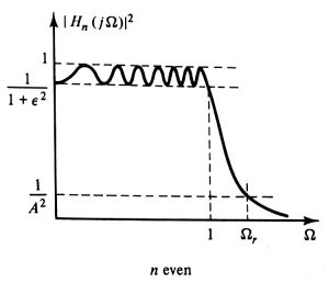
This curve is shown for a normalized even-order (n) low pass filter whose cut-off frequency is 1 rad/s.

First, I’m going to select the stop frequency to be the Nyquist frequency of the standard CD audio sampling rate of 44.1 kHz, so let Ωr = 22000 * 2π rad/s.

Next, the cut-off frequency (at which the linear gain is equal to 1/(1+ϵ^2)) needs to be selected. The lower the cut-off frequency, the less sharp the transition between the cut-off and stop bands, the lower the filter order, and the simpler the circuit. So this should be set as low as reasonably possible. Even though humans can hear sounds as high as 20 kHz (depending on the person), most commonly encountered sounds exist below 12 kHz as shown by this frequency plot of various common sounds. Why 12 kHz instead of 10 or 14? This is where I’m making an educated guess in balancing the need to capture the desired frequency content against the need to not build an overly complicated filter circuit. So, I selected 12 kHz for the cut-off frequency; this means the 1 rad/s cut-off frequency shown in the above Chebyshev response curve will be scaled to 12000 * 2π rad/s (as per the low-pass to low-pass filter transformation described in Chapter 3 of Ludeman’s textbook cited above).

Now let’s select the maximum passband ripple. The Chebyshev response allows us to have a sharper transition from pass to stop band if we’re willing to accept more passband ripple. In this application, let’s set a maximum 10% reduction in the signal magnitude in the passband; this corresponds to 1 dB of allowable passband ripple. As per the ideal Chebyshev response curve above, the passband ripple is the same as the attenuation at the cut-off frequency. So, by choosing a 1 dB passband ripple, the attenuation at the cut-off frequency will be 1 dB as well.

As for the filter order, let’s select a 4th order filter mainly out of convenience: since many op-amp ICs are two op-amps in one, we can realize two 2nd-order filter stages using one IC.

At this point, all the response parameters are defined except for the stopband attenuation (1/A^2). Based on the equations 3.27 and 3.28 given in chapter 3 of Ludeman’s textbook, one can calculate the required filter order to realize a given set of Chebyshev filter specifications. In our case, we want the filter order to be no larger than n = 4, so instead we’ll calculate the largest stopband attenuation that can be achieved given the rest of the filter parameters. So for a 4th order Chebyshev filter with 1 dB passband ripple, 12 kHz cutoff, and 22 kHz stop frequency, the highest achievable stopband attenuation is 30 dB.

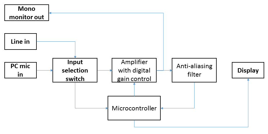
30 dB corresponds to a linear gain of at most 0.032 V/V at 22 kHz (a gain that only decreases as the frequency increases beyond 22 kHz). The ADC on the TIVA LaunchPad has only 12 bits of resolution distributed between 0 and 3.3 V, which means any unwanted signal due to aliasing needs to be attenuated enough to fit within the 0.8 mV quantization step size of the ADC – in other words, unwanted signal with an amplitude of less than 0.4 mV at the ADC input will, for the most part, not be included in the digital representation of the signal. Now the big unknown is the strength of the noise at and above 22 kHz. Though I don’t know how much noise to expect until the circuit is built, with a 30 dB attenuation at the beginning of the stop band, the largest signal voltage that could be more-or-less “hidden” from the ADC, if applied before the filter, would be 12 mV. This will be handy to know to prepare for the possibility of troubleshooting noise problems in the actual circuit.

Selecting a filter topology

We need an active filter topology to realize this Chebyshev filter. Though there are several options available, I’m going to narrow it down to the simplest two options: the Sallen-Key and Multiple Feedback (MFB) topologies. At first, based on this video overview of the two topologies, it seems like Sallen-Key is a good choice since it is less noisy than the MFB. Yet further searching reveals someone’s question regarding the noise properties of the two topologies, and the guy in that video actually answers the question to clarify that the noise gain of the Sallen-Key starts to increase at the “mid frequencies” while the MFB noise gain decreases as frequency increases. This, combined with the fact that the Sallen-Key starts to pass very high frequencies after a certain point, leads me to select the MFB topology for this application.

(Of course, if this were not a hobby project and more were riding on the filter’s performance, I would conduct a more in-depth analysis and perhaps even implement the filter using both topologies and compare the performance, but I believe that would be overkill for what I’m trying to do here.)

Calculating the component values

The MFB topology has one other handy property: its transfer function has the same form as the Chebyshev response transfer function, which basically means that its component values can be calculated such that the resulting electronic filter will have a Chebyshev response. So, we can read the required transfer function coefficients from Tables 3.4 and 3.5 from Ludeman’s analog filter design chapter, and then set these equal to the corresponding coefficients in the MFB topology transfer function. Since the MFB transfer function is written in terms of its component (resistor and capacitor) values, it becomes a matter of resolving a system of equations.

By this point I had put the entire design procedure into a spreadsheet (Filter_Design_4thOrder_MFB_Chebyshev_foronline), and proceeded to determine the component values using guess and check while only “guessing” using values from tables of standard resistor and capacitor values. This way, I can obtain reasonable resistances and capacitances that can be purchased in a single reasonably-sized component.

Simulating the filter

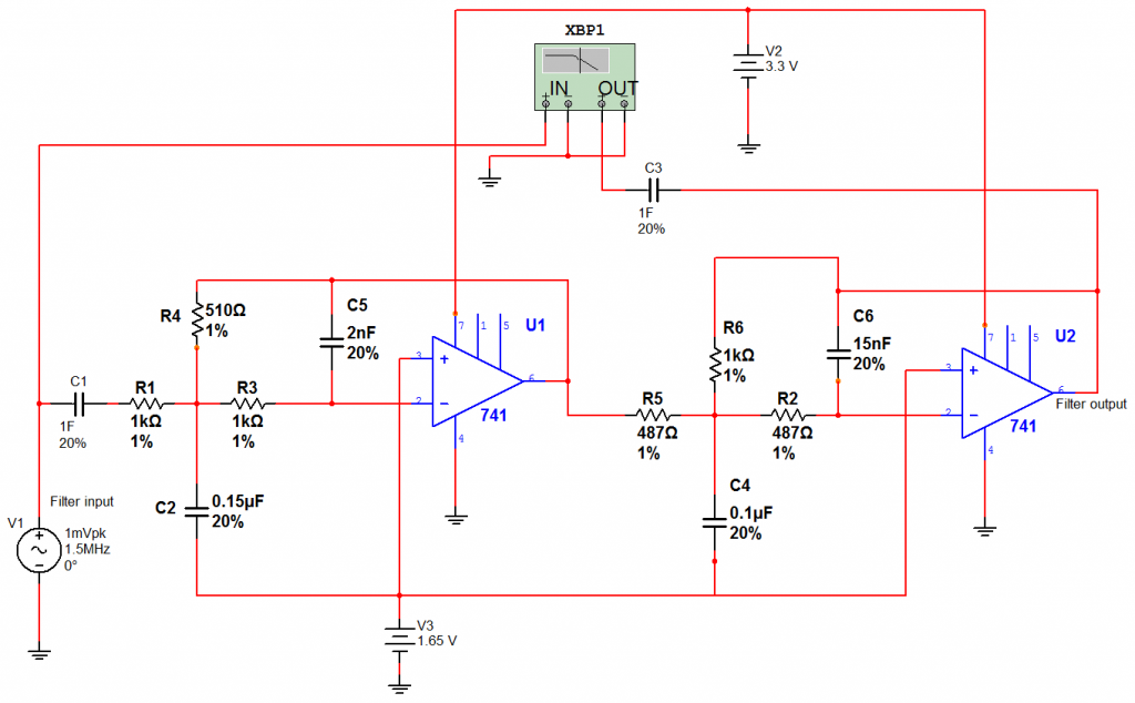
Using Multisim I simulated the resulting two stage filter. In particular, I’m using a unipolar design as I won’t have -3.3 V available to me, so the input signal gets biased to half the supply voltage (half of 3.3 V, or 1.65 V). The 1 F capacitors at the input and output stages will be replaced by a more realistic value when I build the circuit, but for now they are placeholders that won’t affect the simulated low frequency response. Here’s the schematic I drew in Multisim:

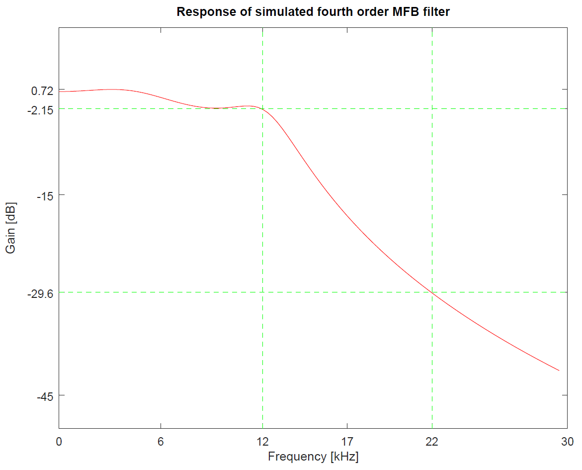
The XBP1 component is a virtual instrument that makes Bode plots. Here is the frequency plot generated by XB1 representing the response of the simulated filter (plotted in Octave):

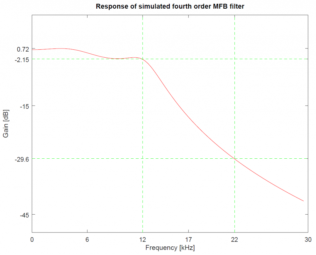
It turns out that, with the selected real-world component values, as well as whatever non-ideal model parameters Multisim takes into account for the 741 op-amp, the response is somewhat less ideal compared to what we would expect from the theoretical Chebyshev response curve. We do get a 1 dB passband ripple, but only up to about 6 kHz, while 6 to 12 kHz sees an additional 2 dB drop, resulting in a cumulative 3 dB attenuation by the time we get to the 12 kHz cut-off frequency. So I ask for a 1 dB passband ripple, but get 3 dB instead. A 3 dB attenuation corresponds to a maximum 29% decrease in signal amplitude. As mentioned in a previous post, passband flatness is not necessary because the bispectrum does not care as much about the relative magnitude of the signals in the passband; for this reason, the cumulative 3 dB attenuation (up to 29% decrease in signal amplitude) at the cut-off frequency (12 kHz) is acceptable for the application. Luckily, the stop band, which starts at 22 kHz, has the 30 dB attenuation I requested. This filter response is adequate for the bispectrum visualizer, so this design step is complete.

Hardware specification part I: microcontroller and display

Before continuing work on the system subcomponents, I’m going to specify two basic hardware components: the microcontroller and the display.

Microcontroller

First, for the microcontroller, I will use the TIVA LaunchPad (TM4C123GXL) as the foundation on which to build the Bispectrum Visualizer. Why? It provides a fast (75 MHz) 32 bit CPU with DSP-like capability thanks to its multiply-accumulate register. It also supports in-circuit debugging via its USB interface, is supported by good software libraries and development tools, and most importantly, I already have experience with the TIVA LaunchPad. Its 32 kb of RAM is rather constrained for the matrices of values that will represent the bispectra, but this will make the firmware design more interesting as a learning experience.

The TIVA LaunchPad provides headers to connect external circuitry. My plan is to design a PCB that fits into this header that implements all of the audio circuitry, including audio connectors, amplifier, and filter.

The board runs from a 3.3 V regulated supply that can drive up to 500 mA with overcurrent protection, powered by 5 V from a micro USB connection. This means the ADC of the onboard microcontroller will be able to digitize voltages in the range of 0 to 3.3 V – important to know when designing the amplifier and filter electronics.

Display

And finally, for the display, I will use an existing display module already designed to connect to the TIVA LaunchPad, the Kentec QVGA Display BoosterPack (BOOSTXL-K350QVG-S1). Specifying this display now is important because it will define which header pins are free to use for my own circuit.

Anti-aliasing filter design part I: filter response

This post describes the rationale for selecting the magnitude and phase response of the anti-aliasing filter. (The hardware block diagram shows how this filter fits into the overall system.)

Phase response

The phase response of the filter – i.e. the relative time delay applied to each frequency – does not matter as far as the bispectrum is concerned. As I wrote in “A better definition of the bispectrum“, the bispectrum only depends on the relative phase between the signal frequencies f1, f2, and (f1 + f2) when bispectra are averaged and normalized. When the relative phase between these frequency components is constant across the averaged bispectra, the bispectrum is “hot”; when the phase between the components is not constant (i.e. random), it is “cold”. If the original signal is put through a filter prior to the calculation of the bispectrum, each of the frequency components f1, f2, and (f1 + f2) will undergo phase shifts of ϕ1, ϕ2, and ϕ3, respectively; each of these phase shifts will be constant because the bispectrum is independently calculated at every frequency triplet (f1, f2, f1 + f2). So whether the relative phases between frequency components are constant or random in the original signal, adding an unspecified but constant phase shift to each of these frequency components will not affect their phase differences with respect to one another. For this reason, the bispectrum is indifferent to the phase response of the filter. (Within reason of course – if a very long phase delay of 1 second existed in the filter, that would be a problem.)

So the phase response of the anti-aliasing filter need not be flat, despite the bispectrum depending heavily on the phase information present within the signal. Not having a strict requirement on the phase response actually helps us obtain a more desirable magnitude response, as explained in the next section.

Magnitude response

Let’s start with the fundamental response requirement. The anti-aliasing filter should ideally prevent all frequencies in an analog signal that are higher than half the sampling rate from reaching the analog-to-digital converter (ADC). So, we want a low pass type of magnitude response.

Next, let’s choose a particular shape for the low-pass response. I’m going to limit the options to what can be realized with an active filter. Since there will already be a power source in the system, it doesn’t take much additional work to get the benefits of an active filter compared to a passive filter.

This page provides a good introduction to the advantages and disadvantages of the four basic active filter responses. The Bessel, Butterworth, Chebyshev, and Elliptic responses provide progressively steeper roll-off in the transition band. But choosing a response with a steeper roll-off comes at the cost of a less flat phase response as well as progressively greater ripples in the pass and/or stop bands. Since we already know that a flat phase response is not needed, a response with a steeper roll-off can be chosen. Since a steeper roll-off can be achieved, the filter need not have as many components (have as high an order) than if the Bessel or Butterworth responses were used.

The Elliptic response would appear to be a good choice. The Elliptic response, however, has ripples in both the pass and stop bands. I’m willing to accept some ripples in the pass band, only because the bispectrum can probably tolerate some magnitude inaccuracy since the signal magnitude is a secondary determinant of bispectrum magnitude (the primary determinant is the relative phase relationships between frequency components). For the stop band, however, I want uniform attenuation because I don’t want to allow the potential for aliasing at much lower frequencies due to a decrease in stopband attenuation. The Chebyshev filter gives us a flat stopband and an adjustable level of ripple in the pass band. Allowing greater ripple in the pass band allows for a sharper cut-off, so this parameter can be adjusted to permit a trade-off between steepness and passband ripple.

To summarize, an anti-aliasing filter with a Chebyshev response is probably the best fit for the bispectrum visualizer because:

  • It has the sharpest possible roll-off while keeping a flat response in the stopband. This allows me to build a simpler filter with less components.
  • Its passband ripple can be adjusted to strike a balance between the sharpness of the roll-off versus passband ripple.

Next filter design steps

In a sequel post I will define the Chebyshev response parameters, such as passband ripple, cut-off frequency, stop frequency, and stopband attenuation, as well as determine the necessary filter order. In the same post I hope to select an existing electronic filter topology, select the components to obtain the desired response, and simulate the circuit to verify its performance.

Hardware block diagram

Here’s the hardware block diagram for the Bispectrum Visualizer, which shows the “big picture” approach to the hardware implementation.

Let’s start with the external facing subcomponents (in boldface). The device will have two audio input connectors: one for a microphone, and another for a line-level audio source. This will allow the system to display the bispectrum of live sounds in the environment, or from a pre-recorded source, such as a personal music player. A switch will be used to define which input source (microphone or line in) is used to compute the bispectrum. A mono monitor out is provided so that inputs may be optionally monitored or recorded by an external device. A display is included, of course, to display the bispectrum.

The most important internal analog subcomponents are the amplifier and anti-aliasing filter. The gain of the amplifier will be controlled by the microcontroller at minimum according to which input is selected, and perhaps also according to whether clipping is detected in the digitized audio stream. The anti-aliasing filter prevents frequencies above the Nyquist frequency from being “reflected” (or aliased) to lower frequencies, corrupting the signal at the frequencies of interest. And finally, the microcontroller will contain the analog-to-digital converter, memory, and signal processing firmware to compute the bispectrum and send it to the display.

A better definition of the bispectrum (revised Dec 18)

In the last entry I wrote about attempting to understand the bispectrum on an intuitive level by building a piece of hardware to display the bispectrum. It turns out, however, that there are some important mathematical aspects of the bispectrum to take into account in order to best design a system that can acquire a signal and display its bispectrum.

In my first post I plotted a bispectrum. The method I used to calculate the bispectrum, while not incorrect, doesn’t do the bispectrum justice. What I had done to make the plot in my last entry was first calculate the discrete fourier transform F(f) of the signal. Then, at each pair of frequency bins (f1, f2), I multiplied only the magnitudes |F(f1)|, |F(f2)|, and |F*(f1 + f2)| and plotted the result. All this really did is create “hot” (red) spots wherever the product of the signal amplitude is large at each of the frequencies f1, f2, and f1 + f2.

Taking into account the phase of the signal

Taking into account the phase information /_F(f), however, really lets the bispectrum shine. To understand this, we need to look at the definition of the bispectrum (from Wikipedia):

B(f1, f2) = F(f1) F(f2) F*(f1 + f2)

If we take a cue from power spectrum estimation techniques and use Welch’s method to estimate the bispectrum by averaging the complex bispectrum calculated from overlapped windowed segments of the signal, then destructive or constructive interference of the bispectral quantity is possible. This means if we apply the averaging implied by Welch’s method, then the frequency pair (f1,f2) will show up as “hot” on the bispectrum plot when the phase of the sinusoids at each of the three frequencies f1, f2, and f1 + f2 add up to the same constant value over all the windowed segements of the signal. A detailed explanation of how the components can sum or cancel is available on Wikipedia’s page for Bicoherence.

Wait… Bicoherence?

It turns out that if you average a bispectrum in the manner I described above and you normalize it, you’ve actually calculated the bicoherence. Ultimately, however, you’re still calculating a bispectrum. To keep things simple, I will continue to use the term bispectrum rather than bicoherence.

I re-did the plot from my last post with this new approach, as shown below. (For those who are interested, there is 50% overlap between windows 1024 samples long, and a Blackman window applied. Normalization is performed by taking the absolute sum of the bispectra divided by the sum of the absolute bispectra.)

This is certainly different from the previous bispectrum. In fact, all of the hot spots on the previous plot are no longer present in the above plot. This alternate method of averaging many bispectra should be used in the firmware of the Bispectrum Visualizer to take advantage of the phase information present in the signal.

Introduction: What is the bispectrum?

The bispectrum is a tool for analyzing signals. While the power spectrum of a signal breaks down the power of a signal by its frequency, the bispectrum provides information regarding specific interactions between the various frequency components of a signal. What can this tell us? Various sources, such as Wikipedia, researchers in Japan and the UK, and academic articles say that the bispectrum can tell us about the nonlinear interactions in a process that generates a signal. These are great articles – full of precise mathematics and deep technical detail. But after reading these sources, I don’t understand, on a simple and intuitive level, how the bispectrum of a signal really represents a signal.

Various web searches did not reveal sources with a truly intuitive explanation. Maybe the bispectrum can’t be explained or demonstrated in simple terms at all – math might very well be the only way to communicate the concept. But it looks like no one has really tried to explain what the bispectrum is in a simple manner. I must not be the first person who has faced the bispectrum and felt that the mathematical definition leaves more to be desired. The bispectrum appears to live in an academic world. My goal with this project is to bring the concept of the bispectrum within both conceptual and practical reach of a wider audience.

Show, don’t tell

The mathematical definition of the bispecrtum is like a recipe – it defines the operations necessary to produce a bispectrum. It tells you what to do, and once you do it, you get a result that you can plot, and therefore see. Seeing is essential for understanding. So, I recorded an audio signal of myself saying “hello world” and plotted its bispectrum:

This helps a bit, but not much. What do those vertical and diagonal lines indicate? Is it a unique mark of my voice? What about those green puddles between the lines? I don’t know. It would be better if I had a way of quickly generating the bispectrum of various familiar sounds (signals). In particular, real-time generation of the bispectrum would help me develop an intuitive understanding of how a bispectrum represents sound. Then I might be able to go beyond the mathematical definition by showing what a bispectrum really represents.

Build a bispectrum visualizer

A portable instrument that rapidly and repeatedly computes and displays the bispectrum of real-world sounds would provide the best way, I think, to gain an appreciation of how the bispectrum represents a signal. Spectrum analyzers are commercial laboratory instruments that display the power spectrum of an electrical signal and have been built in the “homebrew” context by electronics hobbyists. So why not build my own bispectrum visualizer? (The name “bispectrum analyzer” is already taken by this software.)

Project goals

To build a standalone device with:

  • A standard audio input connector
  • Signal conditioning circuitry
  • A microprocessor to repeatedly compute the bispectrum of the audio signal reasonably quickly
  • A display to show the bispectrum

Looking ahead

Future posts will cover the system block diagram and circuit topology followed by detailed circuit design and component selection. Stay tuned for more!